
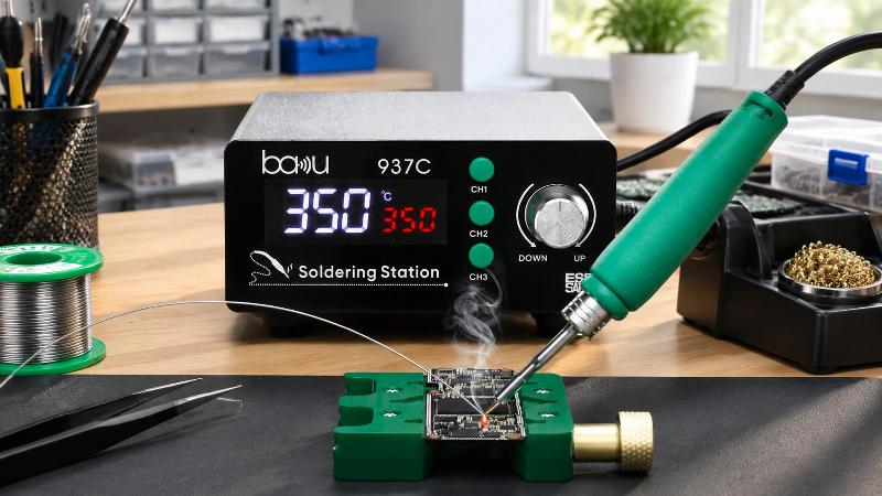
Navigating modern microelectronics assembly demands an intimate understanding of thermal transfer, metallurgy, and equipment architecture. Selecting high-grade electronic soldering equipment is no longer merely a matter of choosing a tool that gets hot enough to melt an alloy wire. Instead, high-density printed circuit boards, microscopic surface-mount footprints, and multi-layer copper planes require surgical heat delivery, careful electrical safety practices, and structural stability. Whether troubleshooting multilayer smartphone logic boards or maintaining industrial control assemblies, choosing suitable professional electronic soldering equipment can support a more controlled, repeatable soldering process, though actual joint quality and IPC acceptability still depend on materials, workmanship, and the applicable acceptance criteria rather than the tool alone. Modern electronics have pushed thermal tolerances to their physical extremes, and a single thermal transient exceeding standard profiles can destroy a silicon die, lift an internal circuit trace, or crack a ceramic capacitor.
To master this discipline, technicians and manufacturing engineers must inspect the underlying heating mechanics, convection physics, mechanical fixturing, and chemical aids that constitute a complete precision rework bench. Each of these elements interacts with the others, so understanding soldering equipment in isolation rarely explains why one repair bench consistently outperforms another on dense, modern boards.
A soldering bench generally combines two heat-delivery methods with one solder-removal method. Direct thermal conduction and forced fluid convection both deliver heat into the joint, with conduction addressing direct terminal bonds and convection managing perimeter joints without mechanical contact. Vacuum-assisted evacuation is a separate function that removes molten solder from a joint rather than delivering heat to it, and desoldering tools apply it to strip liquefied alloy from deep multi-layer barrels. Balancing heat delivery with effective solder removal is essential for reliable board-level operations.
Direct contact soldering stations transfer heat via physical contact between a metallic tip and component leads. Traditional ceramic-core irons separate the heating element, thermal sensor, and interchangeable copper tip. While economical, this separated geometry introduces measurable air gaps and interfacial thermal resistance, creating a delayed feedback loop when a cold solder joint draws heat away from the tip.
In contrast, modern active cartridge systems fuse the heating element, thermocouple, and plating into a single modular unit. By situating the sensor within millimeters of the actual working surface, these cartridges can shorten thermal recovery latency considerably compared with separated-sensor designs, which reduces the temptation to raise dial temperatures simply to compensate for sluggish heat transfer.
Induction-curie heating represents another distinct engineering branch, utilizing high-frequency alternating magnetic fields to excite ferromagnetic tip alloys. These systems inherently self-regulate: once the tip reaches its alloy Curie point, magnetic permeability collapses, reducing power induction without relying solely on conventional software control loops.
Unlike contact irons, convective hot air stations rely on heated gas streams to liquefy multiple termination points simultaneously. These tools are indispensable when dealing with Quad Flat No-Lead packages and Ball Grid Arrays, where contact terminals sit largely concealed beneath the package body rather than exposed along an edge. QFN leads sit at the package perimeter or underside, while BGA connections take the form of solder balls arranged across the base of the package. The primary operational challenge lies in maintaining uniform heat saturation across the target chip without turning adjacent 0201 passive components into airborne projectiles.
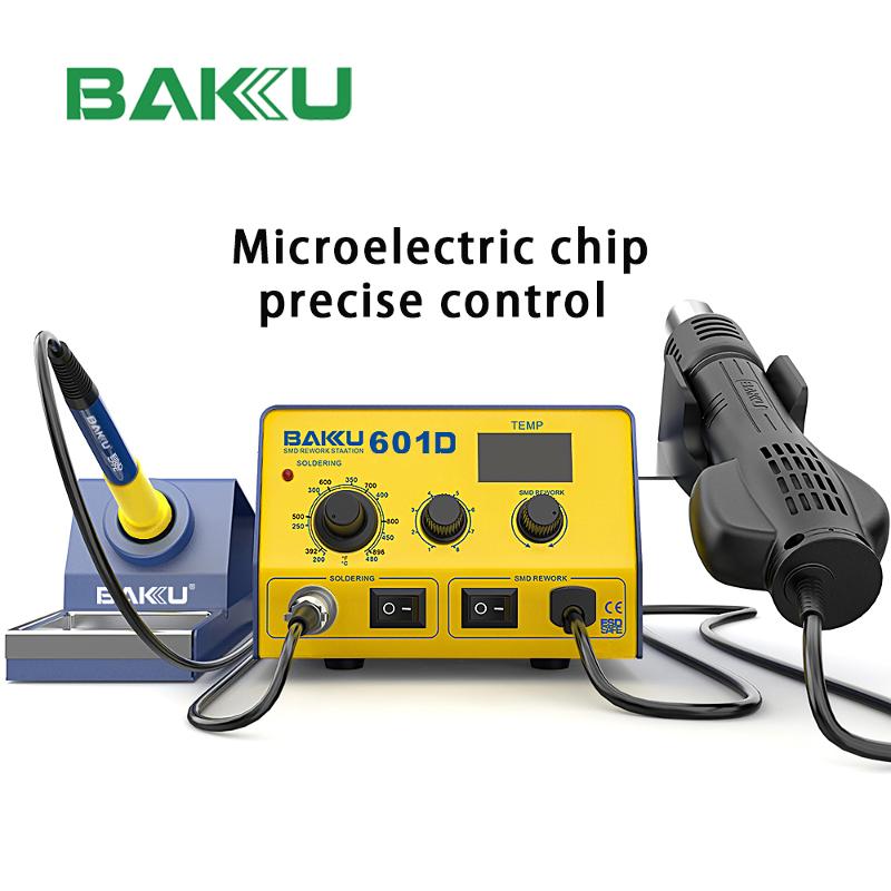
Airflow modulation makes a measurable difference in these scenarios. The supplied specifications for this equipment line list airflow capacity up to 120L/min. Technicians can match broad nozzles and higher airflow volumes to heavy ground-plane boards, or narrow nozzles and gentler laminar streams to dense smartphone layouts.
Plated through-hole components and dense pin-grid arrays demand dedicated solder extraction rather than passive wicking wire. Powered vacuum desoldering stations generally combine a hollow, heated contact tip with a vacuum source that draws molten solder away from the joint once it liquefies; the specific pump arrangement and solder-collection design vary between systems. When applied against a pin, the tip liquefies the fillet within the barrel, and the station’s suction then pulls the liquid metal clear of the hole into its collection chamber.
Using low-cost desoldering braid on fine multi-layer boards carries some practical risk. If the braid is left in contact too long, or if a technician applies excessive downward pressure while dragging it across a pad, the resulting heat and mechanical force can lift or damage delicate pads and traces. Continuous vacuum suction clearing the hole in a short duty cycle reduces this kind of mechanical contact, which can help keep surrounding copper lands intact when heat and pressure are properly controlled.
Solder joints can fail from insufficient heat, excessive heat, or poorly controlled thermal fluctuations in equal measure. Too little heat leaves the alloy only partially melted, so it fails to wet the pad and lead properly, while excessive temperature or prolonged exposure time can thermally degrade the resin in the circuit laminate or contribute to delamination. The real engineering goal in electronic soldering equipment is achieving stable, responsive energy delivery that supplies enough energy for proper wetting while limiting damage to the board and surrounding components, since both extremes of too little heat and too much heat create their own failure modes on dense boards.
Many precision soldering stations rely on proportional-integral-derivative control algorithms embedded in internal microcontrollers, though the exact control scheme varies by manufacturer and model. When a cold copper terminal touches the soldering tip, thermal energy rushes out of the tool, triggering an instantaneous drop in tip temperature, and a passive soldering iron reacts slowly, leaving the technician stuck waiting on an unmelted, sluggish joint.
On stations that use this approach, the controller samples internal thermocouple feedback at a high rate and evaluates both the magnitude and the rate of temperature decline, driving pulse-width modulated power into the heating element to limit how far the tip face drops. The manufacturer states a temperature stability of plus or minus 1 degree Celsius for its precision soldering stations, without specifying the exact measurement point or test conditions behind that figure. This stated stability describes the station’s temperature control behavior rather than a guarantee about the metallurgical structure of any given joint, which also depends on contact time, alloy, and board conditions.
The table below illustrates typical, generalized relationships between control approach and expected thermal behavior; exact figures vary by manufacturer, model, and test method, and should be confirmed against a specific unit’s documentation rather than treated as fixed industry values. The categories describe general tendencies of each control architecture rather than a guaranteed outcome, since setpoint selection, tool condition, calibration, and operator technique all still influence the actual result on the bench.
| Control Method | Typical Temperature Deviation | Typical Recovery Behavior | Commonly Suited Applications |
|---|---|---|---|
| Open-Loop Variable Voltage | Wide swings, varies by load | Slow | Coarse structural wiring, non-sensitive tins |
| Conventional Ceramic Sensor | Moderate swings | Moderate | Single-layer consumer electronics, through-hole |
| Closed-Loop Microprocessor PID | Narrow swings | Fast | Micro-SMD, multi-layer logic boards, BGA balls |
| High-Frequency Induction | Narrow swings | Fast | High-volume industrial manufacturing, demanding builds |
The global electronics industry’s transition to lead-free alloys like SAC305, composed of roughly 96.5% tin, 3.0% silver, and 0.5% copper, compressed the safe processing window for rework. Traditional eutectic tin-lead solder melts around 183℃, allowing operators to run stations at lower baseline temperatures without stressing surrounding plastics or FR4 resin binders.
SAC305 has a melting range of about 217 to 220°C, with a liquidus near 220°C, so iron operating temperatures generally need to run higher to achieve reliable wetting. This elevated thermal baseline tends to accelerate copper tip erosion, speed up surface oxidation, and increase the risk of component delamination if not managed carefully, which means soldering equipment must deliver thermal energy efficiently during brief contact rather than relying on prolonged baseline temperature elevation.
Thermal transfer behaves somewhat like electrical current: heat flow is broadly proportional to contact area and inversely related to thermal boundary resistance. Attempting to solder a heavy ground terminal with a micro-needle conical tip resembles trying to drain a swimming pool through a drinking straw, since the tip’s small contact patch restricts heat flow and causes the operator to wrongly assume the iron lacks sufficient wattage.
Selecting the right tip geometry, such as chisel, bevel, or blade profiles, increases the physical contact area against lead and pad. A wider chisel tip maintains lower thermal interface resistance, transferring heat energy more quickly, which can allow operators to complete joints faster and helps protect sensitive silicon dies from prolonged, deep-soak thermal stress.
Electrostatic discharge represents a largely invisible hazard across the electronics assembly bench. Many electrostatic discharge events go completely unnoticed by the person handling a board, yet modern CMOS transistors and thin-film gate oxides can suffer dielectric breakdown from discharges in the tens of volts. Because human perception is not a reliable indicator of ESD risk, professional tools should be built with static accumulation in mind rather than relying on whether a technician can feel a shock.
ESD control programs for electronics manufacturing and repair facilities are commonly organized around ANSI/ESD S20.20, which addresses overall facility and workstation controls such as grounding, flooring, and ionization rather than specifying tip-level electrical limits for individual tools. Test methods for soldering and desoldering hand tools, including tip-to-ground resistance, voltage, and leakage current, fall under separate ESD Association hand-tool test standards such as ANSI/ESD S13.1.
For electronic soldering equipment, this distinction matters in practice. A facility ESD program governs how the workstation as a whole is grounded and controlled, while hand-tool test methods define how an individual soldering iron or desoldering tool should be evaluated for tip-to-ground resistance and leakage. Specific pass or fail thresholds depend on the particular test method and the equipment manufacturer’s documentation rather than a single universal number, so technicians should consult the relevant standard and the tool’s own specifications when verifying compliance.
Surfaces that an operator or a board regularly contacts during rework, such as station housings, hot air handle grips, and handpiece cords, are the parts of a setup most likely to accumulate or transfer static charge, which is why many manufacturers construct them from static-dissipative materials as part of a broader ESD-control program. Insulative plastics can hold localized surface charges for extended periods, creating capacitive discharge hazards whenever they brush past sensitive assemblies.
Dissipative housings are generally designed to drain accumulated static charges toward earth ground at a controlled rate rather than releasing them as sudden sparks, and treating these surfaces is one element of a facility’s overall ESD-control program rather than a universal requirement applied independently to every tool. The supplied specifications for this equipment line describe ESD-safe design elements along with overload protection and auto-sleep functions intended to protect delicate electronic components, and heat-resistant cord materials on handpieces also reduce the risk of insulation damage from incidental contact with a hot tip.
A soldering iron and hot air station cannot operate in isolation. Micro-soldering and board rework require an integrated ecosystem of auxiliary equipment to position assemblies, maintain board flatness, dismantle enclosures, and chemically prepare metallic interfaces. Skimping on auxiliary tooling undermines the precision of even the most sophisticated soldering station.
Directing heated air toward a multi-layer logic board introduces strong localized thermal gradients. Standard metal clamping vises can act as unintentional heat sinks, draining thermal energy away from the repair zone, and thin, unsupported circuit boards may also flex under localized expansion if they are not adequately supported during rework.
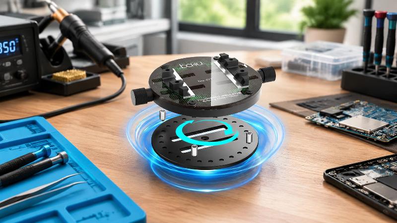
The supplied specifications describe a repair fixture that incorporates a toughened glass platform rated to withstand temperatures up to 500℃, with a clamping range spanning roughly 10mm to 72mm to accommodate boards of different sizes. The rotating, 360-degree design is intended to let technicians reposition a clamped board and approach pin arrays from multiple angles under a stereo microscope, while the stated heat resistance is meant to support safe handling during hot air rework. The manufacturer’s specifications do not detail the extent to which the glass surface redirects or contains airflow during rework.
Repairing modern sealed mobile electronics requires delicate mechanical access before soldering can even begin. Structural adhesives, tight interlocks, and micro-fasteners demand dedicated separation tools that protect fragile components from blunt-force damage.
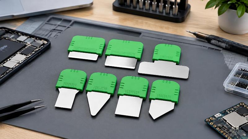
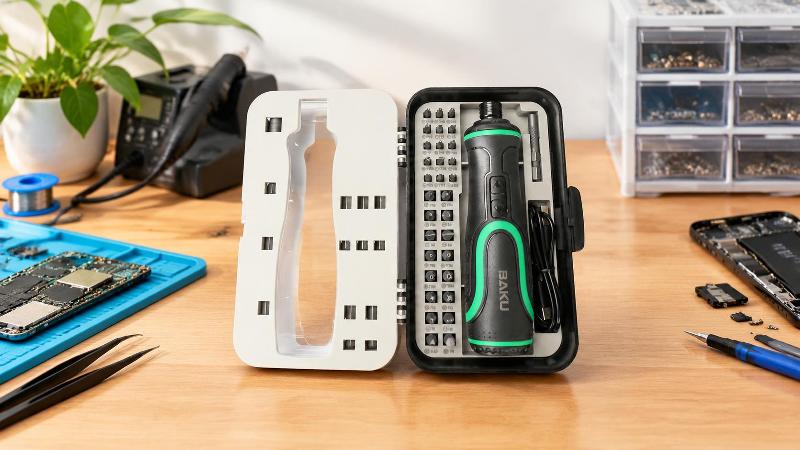
Ultra-thin pry tools with blade thicknesses in the 0.1mm to 0.2mm range, as specified in the product data for this equipment line, can slip into tight housing gaps without gouging aluminum frames or cracking glass backplates. Ergonomic, silicone-wrapped handles help prevent slipping near delicate lithium-polymer battery packs, and paired with magnetic electric screwdrivers featuring 41-in-1 bit arrays, technicians can extract internal shielding plates and motherboard hold-downs without stripping micro-fasteners or generating mechanical shock.
Soldering is fundamentally a chemical process, not merely a thermal one. Clean copper surfaces develop a microscopic oxide layer almost immediately when exposed to atmospheric oxygen, and if unaddressed, this layer prevents molten solder alloys from wetting the copper substrate, producing brittle, rounded solder balls that lack mechanical and electrical integrity.
Chemical flux pastes help remove or suppress this oxide barrier at elevated temperatures, which promotes better wetting between the molten alloy and the copper surface. Rosin-based and synthetic no-clean fluxes are formulated to support this wetting action beneath low-clearance IC packages. The supplied product data describes a BGA solder paste and flux kit supplied as a two-part set, without listing specific particle-size grading or alloy composition details for the paste itself.
Selecting appropriate rework and assembly tooling requires matching equipment capabilities to the thermal mass and pitch density of your target devices. Different production scales and repair environments present unique operational challenges.
For more than 20 years, Baku has designed professional soldering equipment and precision repair tools for mobile phones, computers, and complex electronics; the following evaluation pathways reflect common engineering demands across three typical use cases drawn from that repair industry background.
Smartphone logic boards pack thousands of components into tight, stacked board architectures. The operational challenges here center on confined spaces and thermal vulnerability, since technicians frequently need to replace 01005 passives or reconstruct torn pads under high-magnification optics.
Select a micro-soldering station with active cartridge tips, digital LED readouts, and closed-loop stability within a tight tolerance such as plus or minus 1 degree Celsius.
Choose a hot air unit with fine airflow tuning, interchangeable micro-nozzles, and an auto-sleep function to minimize idling wear.
Implement a 360-degree rotating fixture with a heat-resistant glass base to securely position micro-boards under optical equipment.
Use an appropriate tacky flux to support solder wetting, along with fine curved tweezers to position jumper wire or small components during trace repair.
Industrial motor drives, power inverter boards, and server power supplies present the opposite thermal challenge: massive, thick copper ground planes. Touching a standard iron to these terminals dissipates heat quickly into the board substrate, chilling the joint before the solder can wet the pad.
Deploy higher-wattage contact soldering systems paired with wide chisel or wedge tips suited to larger thermal loads.
Incorporate an under-board infrared or convective preheating plate to raise the entire PCB substrate to a moderate temperature before attempting local soldering.
Utilize motorized vacuum desoldering stations with continuous suction to clean through-hole pin matrices without damaging surrounding barrels.
Avoid fine needle tips, which generally lack the thermal mass needed to overcome the cooling effect of heavy copper planes.
Engineering prototyping benches handle a broad mix of tasks, from assembling through-hole headers to swapping standard QFP components. Versatility, workspace footprint, and budget efficiency are paramount here.
Choose a combination rework station integrating a contact soldering iron and convective hot air wand into a single compact housing.
Confirm the iron accepts affordable, widely available interchangeable tips, including conical, bevel, and chisel geometries.
Select a hot air blower providing airflow up to roughly 120L/min, ensuring sufficient capacity for both small SMD chips and heat-shrink tubing.
Equip the bench with a multi-bit torque driver kit and stainless pry tools to prepare technicians for diverse field-service enclosures.
High-end soldering equipment cannot deliver its designed accuracy if maintenance routines are neglected. Iron tips are not solid chunks of copper; they are precision-engineered, multi-metal laminates. A copper core handles thermal conductivity, an electroplated iron barrier resists solder erosion, a nickel layer helps prevent dewetting, and a chrome outer shell helps stop solder from creeping up the shaft.
The iron plating layer is particularly vulnerable to high-temperature oxidation. When left bare at high operating temperatures, oxygen combines with iron to form an insulative oxide crust that repels solder alloys, and technicians sometimes mistake an oxidized tip for a failed heating element, because molten solder simply balls up and rolls off instead of wetting the surface.
Avoid wiping a tip completely clean before returning it to the stand; flooding the working face with fresh solder helps form a protective sacrificial barrier.
Use dry brass wire cleaning curls rather than wet cellulose sponges, since dry cleaning avoids introducing moisture and the sudden cooling that a wet sponge can bring to a hot tip.
Apply chemical tip activator pastes at modest temperatures to help strip away stubborn, built-up oxide films.
Avoid scraping tips with mechanical abrasives, files, or emery cloth, as cutting through the thin iron shell exposes the inner copper core to rapid erosion.
Over hundreds of operational hours, thermal cycling can alter the internal electrical characteristics of heating elements and thermocouples, so a station display reading 350℃ may, in practice, produce a somewhat different temperature at the tip face. Operating with uncalibrated tools invites cold solder joints or component overheating.
Quality equipment often includes integrated temperature offset calibration functions. Technicians apply fresh solder to a dedicated cross-wire thermocouple thermometer, press the tip firmly against the sensor, and read the stabilized temperature, then input any observed delta into the station’s calibration mode, aligning the digital display with actual tip surface temperatures.
Wattage indicates raw power consumption under full electrical load, but it does not by itself dictate how effectively energy moves into a cold joint. An open-loop iron rated at a given wattage with a loose, poorly fitted tip can experience significant interface losses, leading to slow thermal recovery during demanding joints. A well-designed active-cartridge system places its thermal sensor close to the joint, transferring energy more directly. Thermal recovery rate measures how quickly the tip returns to its set point under load, which is often more meaningful for joint quality than nominal wattage alone.
Precision microelectronics operate within tight structural margins. FR4 laminates can degrade, and circuit traces can lift from the substrate if local temperatures exceed target profiles for extended periods. A tool with wide temperature swings forces technicians to raise their baseline setting higher than necessary simply to prevent tip-freezing during contact. A tighter stated stability, such as the plus or minus 1 degree Celsius figure given for this equipment line’s precision stations, describes the station’s own temperature control and can make it easier to work nearer the lower end of an alloy’s melting range, though the actual condition of a finished joint still depends on contact time, heat capacity, and board materials.
Lead-free alloys like SAC305 contain roughly 96.5% tin, compared to about 63% in traditional leaded solders. At the higher working temperatures these alloys require, molten tin can dissolve iron through intermetallic leaching more readily. Because the protective iron barrier over the copper core is thin, high-tin formulations tend to erode this shielding layer faster than leaded alloys did. This generally makes regular tip tinning, brass curl cleaning, and conservative idle temperatures important for tool longevity.
There is no single universal airflow setting, but rework practice generally favors starting with lower flow rates using a fitted nozzle that channels heat onto the BGA chip perimeter rather than the surrounding area. Broad, unshielded airflow at higher volumes across a densely packed smartphone board risks heating neighboring small passive components past their melting point, which can cause turbulent air to dislodge them from their pads. Once the target package reflows, gentle mechanical extraction with vacuum tweezers helps keep surrounding components undisturbed. Equipment offering adjustable airflow up to 120L/min, as noted in the supplied specifications, gives technicians room to scale output to the task.
Aluminum has high thermal conductivity, which can turn solid metal holding jaws into heat sinks that draw energy away from the circuit board during rework. Technicians sometimes compensate by raising hot air gun temperatures to counteract this loss. Fixtures built with toughened glass platforms, rated in the supplied data to withstand heat up to 500℃, generally have different thermal transfer characteristics than solid aluminum jaws, though the practical effect on board warping or heat distribution during a specific repair depends on fixture design, airflow settings, and overall process control rather than the glass material alone.
High-yield electronics repair and manufacturing are shaped by the practical realities of thermodynamics and materials science. Achieving consistent, high-integrity joints on complex multi-layer boards requires matching process requirements with well-engineered equipment, from active-cartridge irons designed for tight thermal stability to adjustable hot air blowers, heat-resistant glass fixtures, and ESD-conscious housings, since your equipment ecosystem shapes your rework outcomes even as final results still depend on process control and workmanship.
Viewing electronic soldering equipment as an integrated technical system, rather than a collection of isolated hand tools, helps technicians manage lead-free processing challenges, protect sensitive semiconductors, and restore sophisticated hardware with greater confidence.

Technical Guide to Electronic Soldering Equipment: Thermal Dynamics, Architecture, and Selection Fra
Choosing precision soldering equipment involves balancing heating methods, thermal control, ESD protection, and auxiliary tools for reliable board-level rework.

Digital Microscope Guide for Electronics Repair and Precision Soldering
Choosing a digital microscope for electronics repair means balancing optical zoom, working distance, latency, lighting, and bench stability for accurate rework.

The Engineering Guide to Soldering Equipment: Precision Bench Architecture and Microelectronics Rewo
Choosing soldering equipment with precise thermal control, ESD safety, and proper fixtures reduces board damage and improves rework reliability.

Choosing the Right Electronic Repair Equipment for Professional Service Centers
Professional electronic repair equipment including soldering stations, rework fixtures, and precision tools enables efficient, high-quality device repairs in service centers.
Stereo Microscope Price Guide: What Affects the Cost?
Discover what affects the price of a stereo microscope, including magnification, optical quality, digital features, lighting systems, and build materials. Learn how to choose the right model for electronics repair and precision inspection.
Stereo Microscope Uses: From Science Labs to Electronics Repair
Discover the key applications of stereo microscopes in biology labs, education, micro-soldering, and PCB repair. Learn how 3D magnification improves precision for scientific research and electronics technicians.

STAY CONNECTED